Many electronic devices require user input for setting the application properties. Typical input devices include pushbuttons, potentiometers, and touchscreens. To minimize overall project cost, you may have to select low-range microcontrollers, FPGAs (field-programmable gate arrays), or PLDs (programmable-logic devices). These devices don’t provide a wide range of peripherals and often lack analog-to-digital-conversion capability, which can prove annoying when trying to acquire user input. This Design Idea describes a method for adding a low-end ADC to a single programmable-logic I/O pin. The circuit charges a capacitor through a resistor while measuring the time to charge the capacitor to a certain voltage.
Before each measurement, the capacitor discharges to 0V. A single I/O pin can perform both the discharging and the timing. For an FPGA or a PLD, you can perform a discharge by setting the I/O as an output pin and forcing a zero at that pin. You can charge the capacitor by setting the I/O as an input pin, which gives it a high impedance. The capacitor charges through the potentiometer ().
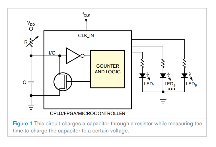
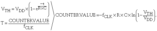
Meanwhile, a counter starts, and the CPLD monitors the input voltage. As soon as the capacitor voltage reaches the threshold, the counter stops at a value that is a measure of the charging time. The charging time or counter value relates to the clock frequency, the value of the resistor, the value of the capacitor, and the input threshold voltage:
If you assume that the capacitor value, the input threshold voltage, and the clock frequency remain fairly constant over the operating range, the charging time is linearly dependent on the value of the resistor. If you replace the resistor with a potentiometer, a counter value depends on the potentiometer position. The application uses a XC9500 XL CPLD ().

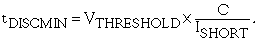
The I/O, which VHDL (very-high-speed-IC hardware-description language) declares as a tristate buffer, first shorts the capacitor. Hardware limits the output short-circuit current of the I/O pins to ±10 mA, so the capacitor’s shorting should last long enough to guarantee a full discharge. You can calculate the minimum shorting time using the capacitor value, short-circuit current, and discharge voltage, assuming that the threshold voltage must discharge from the capacitor:
The discharge delay can be realized with a small counter. After the discharge time, the I/O pin acts as an input, which causes the capacitor to charge through a pullup potentiometer. Meanwhile, the internal counter starts. When the capacitor voltage reaches the input threshold voltage, the counter stops. Eight LEDs show the 8-bit value. In this application, a 10-kΩ potentiometer in series with a 1-kΩ resistor charges a 22-nF capacitor. The input clock of the PLD is 1.8432 MHz. The input threshold is 1.5V at a supply of 3.3V. This arrangement allows a measurement range between a counter value of 25 and 270, equivalent to a resolution of almost 8 bits.
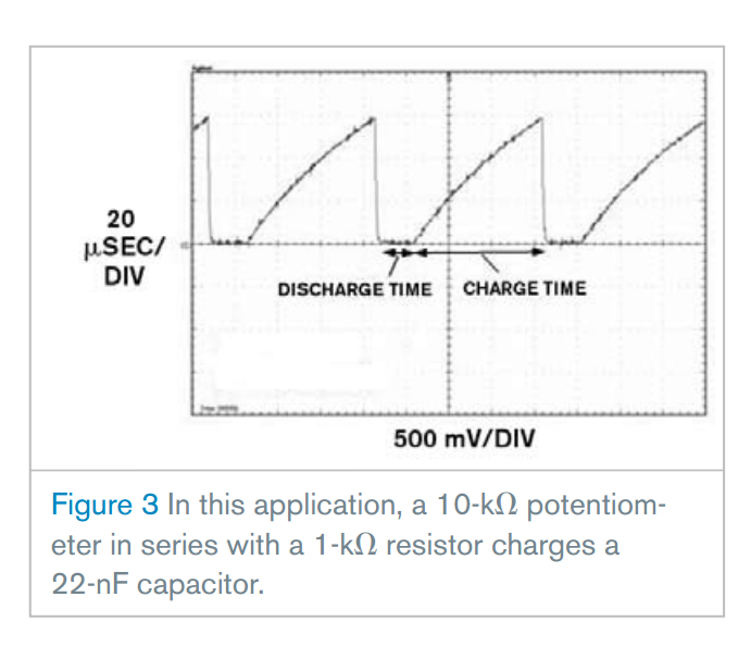
shows the capacitor charging/discharging waveform.
Every IC’s I/O pin has a certain bias sink or source current, causing a voltage drop over the charging resistor. This situation limits the charge voltage to VDD–RCHARGE×IBIAS. In other words, if the charging resistance is too large, the capacitor doesn’t charge above the input-pin threshold voltage, stopping the circuit’s operation. Similar applications for microcontrollers or PLDs () include adding multiple inputs to a single I/O pin and using a different pullup-resistor value for each input. By discriminating the charging times for each resistor, the PLD can decide which resistor or combination of resistors the user has actuated.
Another application for microcontrollers is temperature measurement. By replacing the pullup resistor with a PTC (positive-temperature-coefficient) or an NTC (negative-temperature-coefficient) resistor, you can derive the temperature from the charging time after calibration. You can also use these devices to make true analog-to-digital measurements. By replacing the pullup resistor with a voltage-controlled current source, an input-voltage change causes a linear change in the charging time, providing a real analog-to-digital conversion.
| References |
|